


How Far Can Moore's Law Go?
A modern take on the age old question

Overview
My title is kind of clickbait.
Moore’s Law simply states that the number of transistors on an integrated circuit doubles every 2 years.
My goal is instead to examine what the limits are to computing performance per $, since that’s what we care about at the end of the day.
The goal of this article is to examine what the practical limits to computing are. While there is the possibility of breakthroughs or paradigm shifts, I’ll currently consider only what’s currently been shown so far in literature.
How much further can the cost of compute be practically reduced?
For this I will include both power costs and capital costs of chips.
One common misconception is to simply use the cost of electricity to estimate the cost of power. This is wrong, the fully burdened cost of power includes the electrical and cooling equipment needed to supply that power, which adds an additional cost that is proportional to power.
One thing that I will leave out is architecture. Most of the gains in computing performance in GPUs and AI chips over the last 5 years has been gains in architecture, mostly through specialization. This is outside the scope of this article, since that’s a whole field unto itself :)
TLDR
Power, not transistor density will be the limiter. Transistor density can increase another ~1000X, but you won’t be able to turn those transistors on! (at least not economically)
For parallel workloads like AI:
Gate level: ~10-20X
Chip Level: ~4X
System Level: ~2-5X
Total: ~400X
Limits are meant to be broken, and breakthroughs can change this ;)
Gate, Chip and System Levels
I broadly break improvement categories into three pieces:
Gate Level
Think NAND gates, or a multiplier in an AI chip.
This is primarily transistor focused
Chip Level
Think a GPU, CPU or TPU
This is primarily wire and memory focused
System Level
Think a server w/ 8 GPUs, a cluster with 32,000 GPUs, or a CPU server running a database.
This is primarily memory and networking focused

Gate and chip level, sources: Definition of logic gate | PCMag, Demonstration of Integrated Micro-Electro-Mechanical Relay Circuits for VLSI Applications | IEEE Journals & Magazine
Gate Level
At the gate level:
Although transistor density can increase, you can’t turn those transistors on because they burn too much power.
CMOS density can increase another 100X in 2D
Also in 3D 8-16X, cost starts to increase rapidly after that.
However, power, not transistor density, is the limiter, with ~10X improvements a practical limit
Even if power were free (it’s not), cooling can only tolerate a ~10X increase in power.
Optimistically, a ~10X improvement is possible with current technology, 2X from voltage, 5X from capacitance.
The Boltzmann tyranny sets a ~2X limit to power reduction via voltage reduction
360mV is the limit with current MOSFETs
No sub-Boltzmann limit switch is currently viable
Promising Paths
Breakthroughs in the following could change the game:
A viable sub-Boltzmann limit switch
Nothing appears viable here.
TFETs need at least a 10X speed boost
Severe mismatch between theory and experiment makes progress hard and unpredictable
NC-FETs lack experimental evidence
Cold source FETs suffer from similar issues as TFETs
A viable spintronic device
MESO is promising, but:
Spin <> Charge conversion is too inefficient currently
Magnetoelectric coefficients are too low currently
Low overhead reversible computing
Co-optimizations with devices and/or microarchitecture could make this viable
Currently it does not appear viable
Significant advances in superconducting logic
Would require ALL at once:
Significant miniaturization (~10,000X smaller)
A viable memory device
~100X better cryogenic cooling (or a room temperature superconductor)
Capacitance reduction via 2-D TMDs
There may be a path to gate capacitance reduction here, but there’s no obvious path to parasitic capacitance reduction.
2-D TMDs would allow increased channel control and anisotropic carrier mass, and therefore allow gate lengths to shrink with controllable short channel effects.
Significant advances in cryogenic cooling
On the order of ~100X is needed here, but could reduce the Boltzmann Limit by reducing the T in kT
Summary of scaling vectors:
Capacitance
2X from going to vertical FET
~2-4X from capacitance reduction from dimensional scaling
Voltage:
~2X going from 500mV to 360mV C
Can be done by either eliminating the overdrive voltage, or accepting the speed losses
Chip Level
Since 60-80% of the energy in a chip (even for compute-bound workloads) can go to registers and wires, there’s opportunity for big wins here.
3D Chips
Wire length reduction could offer big benefits
New memories
FeRAM and eDRAM are especially promising
Photonics NoCs
Workload specific optimizations
Eg read-optimized memories, block-level optimized SERDES, etc.
System Level
Utilization for e.g. AI clusters can be as low as 20%, leaving room for 5X, and for some workloads, 10X improvements.
Photonics
Improved networking, reduces costs, boosts compute utilization and reduces cluster power
Disaggregation
Could reduce memory costs
Fault-tolerance
Reduce overhead from spares and time wasted restarting from checkpoints.
Especially important as cluster sizes grow
3D stacked memories
Boost bandwidth, reduce energy costs.
Total: ~200X- game on!
Caveat Emptor
I’m not a device physics expert, or a reversible computing expert, and thus may have made mistakes in my analysis
Please correct me if you see any!
Breakthroughs are rare, but possible!
Many times I’ll say “barring a breakthrough”- they’re rare, but do happen!
“Never bet against humanity”
To paraphrase Warren Buffett. Humans love challenges, and find very creative ways to solve them, especially if money is involved.
“Making predictions is hard, especially about the future” - Yogi Berra
““Thirty-five years ago I was an expert precious-metal quartz-miner. There was an outcrop in my neighborhood that assayed $600 a ton— gold. But every fleck of gold in it was shut up tight and fast in an intractable and impersuadable base-metal shell. Acting as a Consensus, I delivered the final verdict that no human ingenuity would ever be able to set free two dollars’ worth of gold out of a ton of that rock. The fact is, I did not foresee the cyanide process… These sorrows have made me suspicious of Consensuses… I sheer warily off and get behind something, saying to myself, ‘It looks innocent and all right, but no matter, ten to one there’s a cyanide process under that thing somewhere.’”
-Mark Twain, “Dr. Loeb’s Incredible Discovery” (1910)
Workloads
To some extent, the workload, not the hardware limits, sets the performance limits.
Moore’s Law gets us more transistors, but single-threaded CPU workloads generally do not benefit from those transistors in the same way that GPU workloads do!
In fact, CPUs have benefitted very little from the past decade of Moore’s Law.
By contrast, GPUs, and even more, AI accelerators, have benefited tremendously from Moore’s Law over the last decade, leveraging abundant parallelism to throw more transistors at the problem.
There may be opportunities to greatly improve workloads for whom architectures are very far from the gate-level limit, e.g. CPUs.
Disclaimer
This is a personal article, and all of the information here uses public sources, and does not include work and information internal to Volantis or with any vendors or partners we work with.
Gate Level
Transistor Density
Where We Are Now
As of the writing of this article, the state of the art logic technology node is the N3 node, marketed as “3nm”.
We will use TSMC’s N3 as a representative process, since they are the current market leader.
It’s worth noting that TSMC is delaying the transition to GAA-FETs relative to Samsung and is sticking with FinFETs for N3.
Samsung got a penalty in density (relative to TSMC) by switching to GAA-FETs, and when TSMC moves to GAA-FETs, they will also slow down in density scaling.
We have key parameters from TSMC’s N3 disclosure, but not exact gate length (Lg) dimensions. So, we’ll have to guess.
Reasonable guesses for the gate length is ~12-15 nm at the N3 node (Ref. CMOS Scaling, 4, 11).
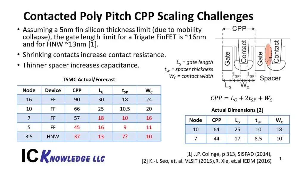
Fig. 1 (Ref. CMOS Scaling, 4)

Fig. 2 (Ref. CMOS Scaling, 11)
Scaling the width down is not ideal due to reduced drive current, so we’ll assume that gate scaling has to happen.
Other aspects like track height reduction, dummy gates, contact over active gate, etc. exist and are important, but we will neglect these for now because we are interested in the limits to scaling. In addition, these “scaling boosters” have already been used, and exhausted to a large extent.
Ok, so assuming a gate length of 12-14nm that has to come down, how far can we go from here?
Planar Scaling
A limit to gate length scaling is predicted by a number of approaches and mechanisms.
Direct S-D Tunneling
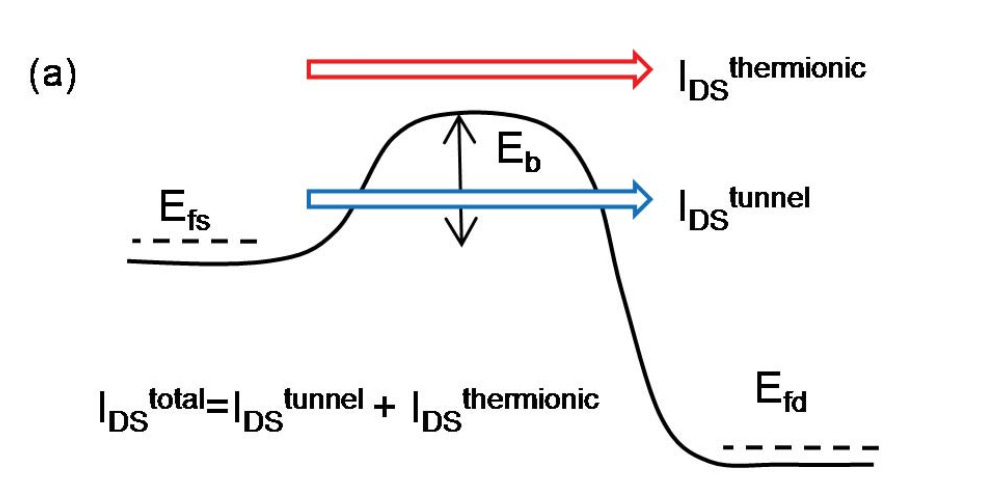
Fig. 3, Source: Ref. CMOS Scaling, Direct S-D Tunneling, 2
In direct source to drain tunneling, carriers tunnel directly from source to drain, bypassing the energy barrier.
This is, unfortunately, quite hard to stop, as it is largely independent of the material.
A number of approaches predict that the practical limit is a gate length of ~5nm (Ref. CMOS Scaling, Direct S-D Tunneling, 1, 2, 3, 4 and CMOS Scaling, 13).
This gives a scaling limit of (12nm/5nm)^2 = ~5.76X smaller than current (estimated) gate lengths at N3.
One option to continue scaling and reduce direct source-drain tunneling issues is to engineer a larger effective carrier mass. This does decrease drive (and make high mobility channels like III-Vs less appealing).
Another option to overcome the ~5 nm limit is to engineer an anisotropic carrier mass (Ref. CMOS Scaling, 2), this effectively squeezes the effective mass so that the tunneling current is greatly reduced.
However, to my understanding, this has been shown in simulation only, not experiment.
Yet another solution is to use Recessed Channel logic transistors (Ref. CMOS Scaling, 1), although this comes at the cost of increased capacitance, and therefore increased power consumption.
In addition, recessed channels will likely not be able to go much below a 5 nm width, especially if high-k dielectrics are used.
Tunneling from gate to source is also a possibility with such a structure (though likely not insurmountable).
Unfortunately, although these approaches may work to allow scaling to continue, they all show a degradation in the subthreshold swing.
As can be seen from Fig, 4, at a gate length of 5 nm, the subthreshold swing degrades to ~100mV/decade. This is already assuming a GAA-FET geometry, and thus channel control improvements from transistor geometry are unlikely.
This would drive power consumption up, and create significant challenges.
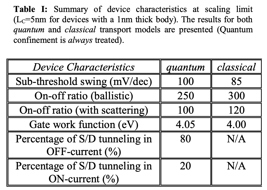
Fig. 4, Source: Ref. CMOS Scaling, Direct S-D Tunneling, 2
Short Channel Effects
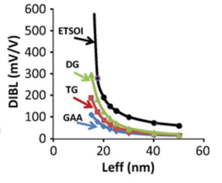
Fig. 5, Source: Ref. CMOS Scaling, 12
From Fig. 5, it can be seen that even with a gate all around geometry, the DIBL continues to go up after the ~15 nm gate length.
Since a further geometry improvement is not possible, this presents a powerful barrier to scaling.
2-D TMDs however, may allow a way around this by a) increasing the control over the channel due to an extremely thin body b) a large effective carrier mass (Ref. Enhanced CMOS, 2D TMD, 1, 2, 3, 4).
Mobility Degradation
Reducing the thickness of a silicon channel beyond ~4nm runs into issues where the channel mobility decreases very rapidly.

Fig. 6, Source: Ref, Main, 4.
Fortunately, 2-D materials allow a way around this, but currently these have severe challenges with low resistance contacts. These issues can likely be overcome however.
“Scaling Boosters”
“Scaling boosters” are approaches that improve the power, performance and area via approaches other than transistor scaling.
Backside PDN, contact over active gate (COAG), active backside (signals as well as power on backside of FEOL), supervias (go down multiple metal stacks with a single via) are all examples.
Unfortunately, by the N2/2 nm node, it is expected that most of these scaling boosters will have been deployed and exhausted (Ref. CMOS Scaling, 4,7,8,9).

Fig. 7, Source: Ref. CMOS Scaling, 15
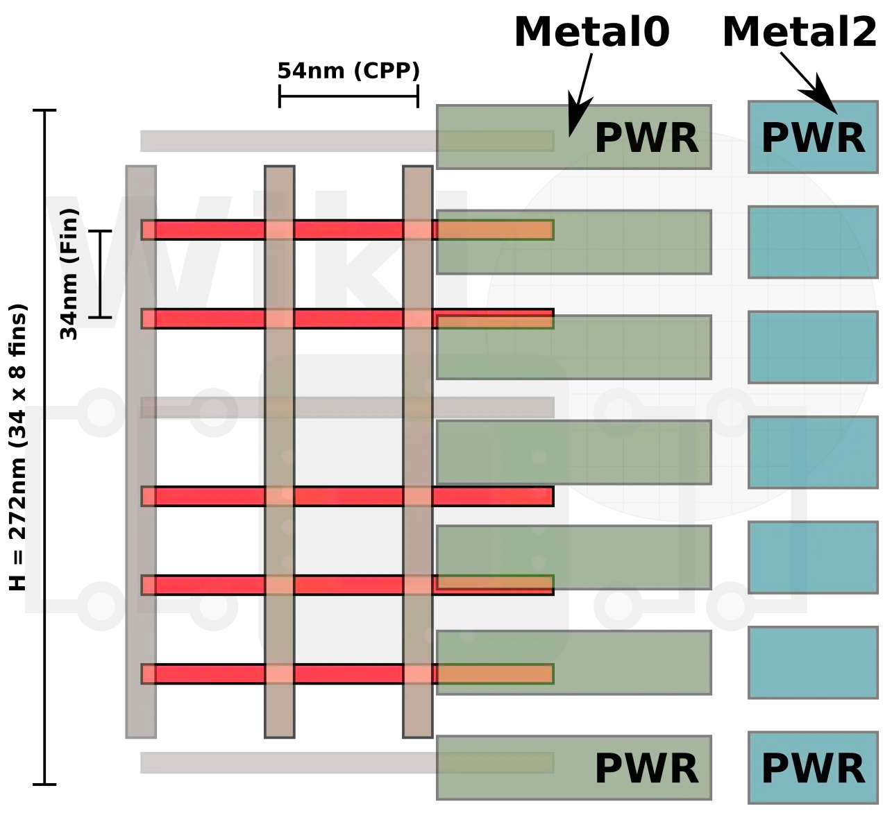
Fig. 8, Source: Ref. CMOS Scaling, 15
One of the most important of these levers is “track height reduction”, which essentially reduces the number of metal tracks and gates in a standard cell. This is important since it reduces the capacitance, reducing power, at the cost of reduced transistor drive. Drive can likely be boosted to compensate, but this lever is also close to exhausted.
Note that smaller track heights also generally increase routing congestion, which presents an obstacle to reducing area and also increases power due to increased metal capacitance.
Vertical FETs
Hopefully the past section has left you with a healthy respect for the challenges of reducing the gate/channel length of MOSFETs.
But, why do all this hard work in the first place?
It seems that you must, since else do you make a transistor smaller?
Why not turn the transistor on its side?!
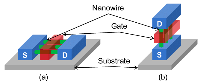
Fig. 9. Source: Ref CMOS Scaling, Vertical FETs, 1
This allows you to greatly reduce the footprint of the transistor, eg for an inverter:

Fig. 10. Source: Ref CMOS Scaling, Vertical FETs, 2
This allows a number of advantages beyond the immediate area footprint reduction:
The gate length can be maintained while scaling continues
This avoids short channel and direct S-D tunneling effects
Also avoids significant mobility degradation since footprint is mostly limited by source/drain size
The parasitic capacitance of the spacer doesn’t go up
Since spacer thickness can remain the same
Potentially greater layout benefits from scaling boosters
Eg backside PDN and monolithic 3D
Offers an alternate path to gate capacitance reduction
Using low DOS materials
SRAM scaling
Allows SRAM scaling to continue
Opportunities for further scaling through new axes
Eg metal S/D with Schottky contacts can allow for the source/drain sizes to be reduced
Ref. CMOS Scaling, 3, 6)
If these approaches can be fully maximized, then a 2 or 4-tier vertical GAA-FET could approach a 6nm 2D footprint, which would represent a ~100X density scaling over today’s N3 node!
3D
Once planar scaling is exhausted, can we start stacking transistors in 3D to increase the density?
There are a few key points here:
Economics
A key point here is that we currently lack a way to add multiple 3D layers of logic transistors (beyond 2-4) and not have the cost go up proportionally.
3D NAND flash like designs may be able to overcome this
It may be possible to reduce costs, but this is reliant upon manufacturing technology we currently do not have (and no roadmap to achieve it).
Thermals
Without proportional power reductions, 3D chip layers will only serve to worsen a thermal problem that is already at the brink (100W/cm^2)
Power delivery
Power delivery systems for high end chips are already strained. Increasing the current draw further will make things worse.
However, this is likely actually solvable, since new approaches like vertical power delivery, integrated voltage regulators, GaN-on-Silicon and backside PDN may allow these issues to be overcome.
So in summary, the economics and practical challenges of 3D chips make it hard to see it significantly improving gate-level performance.
The industry roadmap of CFETs is expected to reduce area by less than 2X (due to routing issues).
However, there are good use cases for 3D chips. 3D register files and 3D integrated memory are both extremely useful at the architecture level (in most systems the majority of the energy is dissipated in the register files and memories).
This is a great example of where the gate-level scaling diverges from architecture level scaling.
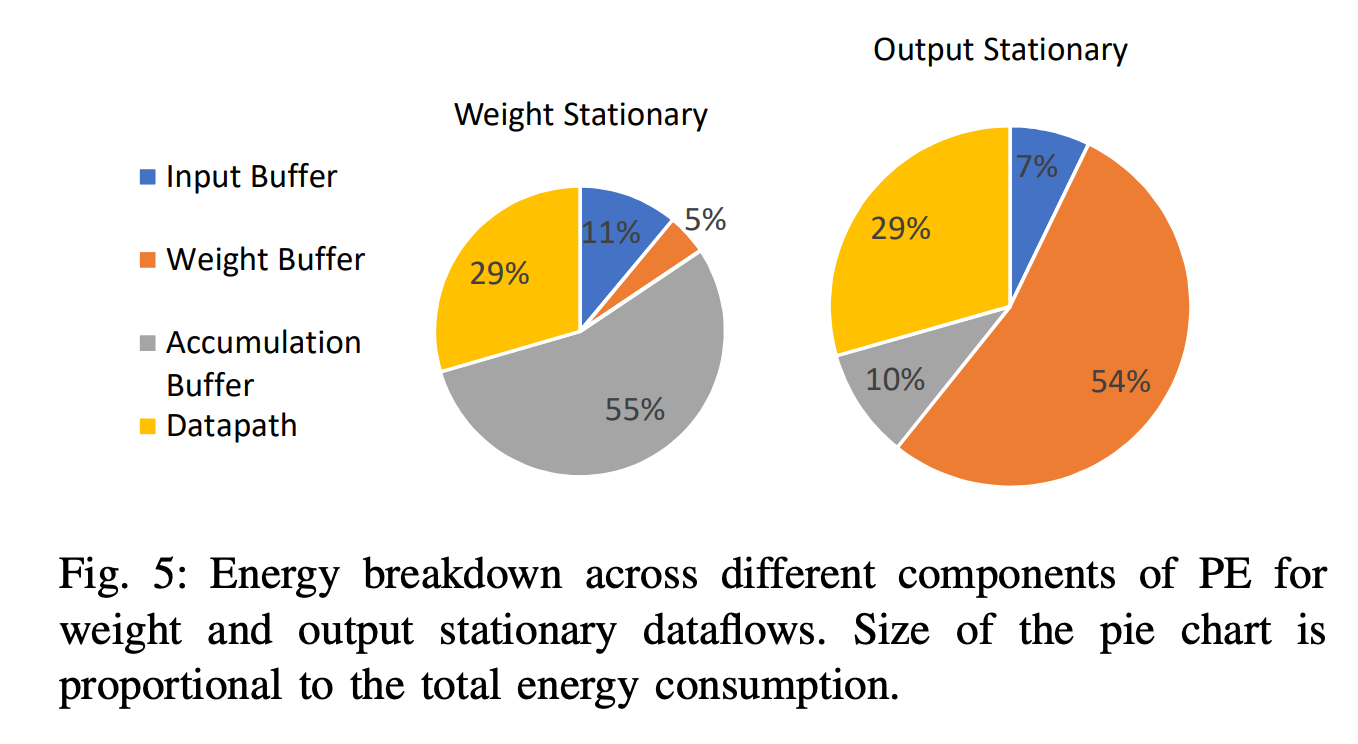
Fig. 11, Source: Ref. System, AI Chips, 1
Fig. 11 is an energy breakdown from a representative AI accelerator for CNNs. Although CNNs are now an outdated workload, it still serves as an example of the benefits that can be gained from 3D chips at the architecture level.
However, as this highlights, even though significant gains can be had at the architecture level from 3D chips, these are likely capped at ~10X.
Power
Given all this, it’s reasonable to expect that density scaling will continue, say up to 100X.
Strictly speaking, this is all Moore’s Law means- that the transistor density goes up (on a given cadence).
So as long as that continues, “Moore’s Law” isn’t dead. But most people are far less interested in how many transistors their chip has, but rather the compute performance that their chip has. And that is the goal of this article, so I’ll look at the impact that transistor density will have on compute performance.
Through that lens, the question becomes: will the cost of compute continue to drop?
Does Power Matter?
Does power even matter to total economics? It’s generally “common wisdom” that power is the dominant cost for compute in the datacenter. As with most “common wisdom”, this is not really true.

Fig 12, source: Ref, Main, 5
Instead, the costs are currently still dominated by the cost of the servers, i.e. hardware capex.
For AI compute this is especially true due to nVidia's extremely high margins, which distorts calculations.
Without Nvidia’s margins, Fig. 12 is generally representative of AI cluster costs (I can’t be more accurate due to conflicts with work at Volantis).
Fully Burdened Power Cost
However, an extremely important point is the “power and cooling infrastructure”. This is the cost of the power delivery equipment and mechanical cooling infrastructure (HVAC, etc.) and scales in proportion to the power. James Hamilton calls this “fully burdened power” (Ref.
Main, 5, 6).
So even in the case where power became free (e.g. due to breakthroughs in nuclear energy), the fully burdened cost of power wouldn’t decrease as much, and costs would continue to be proportional to power draw.
The concept of fully burdened power cost also extends into the chip-level, e.g. DC-DC converters and cooling systems (assuming $100/700W for 48V → 0.5V this is not trivial as TDP goes up).
In some cases the cost of the server capex is much higher than the parameters in Fig. 12, and this does change things quite a bit.
Example applications include certain server nodes where DRAM capacities (and therefore costs) are very high, or AI clusters where nVidia's huge markup (90%+) must be paid.
Nonetheless, in estimating the limits of computing costs, Fig. 12 is directionally correct.
And for other applications, e.g. Bitcoin mining, the power cost is many times the capital cost (~3X opex:capex ratio as a heuristic).
If the lifetime of replacing a chip increases (as it will if chip performance improvements flatline), then the power cost will become even more important, as the 4-year replacement assumption stretches into longer time windows.
It’s possible that advances in power delivery (e.g. GaN and/or switched capacitor converters) and cooling (e.g. supercritical CO2) will bring power infrastructure costs down, but this assumes significant advances.
However, note that this is not impossible!
Cooling
Then there is the problem of cooling.

Fig 13, source: Ref, Main, 7
Way back when (Fig. 13), people realized that the TDP of processors was increasing so quickly that cooling it would be impossible. To counteract this trend, clock speed scaling plateaued.
But how far can cooling performance be pushed?
Current high end processors operate at TDPs of ~100W/cm2 (see e.g. nvidia’s H100). The best known cooling technologies (microfluidics) are in the range of ~1 kW/cm2 (Ref, Main, 8).
Thus, even if fully burdened power were free (and it’s most definitely not with current technology), cooling limits would only allow us another ~10X without needing to reduce power.
Novel approaches like very high flow rate approaches or new materials may change this, but are currently not anticipated.
C*V^2
So then, how much can we reduce power?
The dynamic power of an integrated circuit scales as C*V^2, giving us two levers to reduce power: capacitance and voltage.
Only focusing on dynamic power is optimistic given that leakage is nonzero, but techniques like power gating can actually likely mitigate this, making the optimistic assumption surprisingly feasible.
Capacitance Scaling
Capacitance scaling is hard to discern due to the wide variance between devices, real circuit implementations and the secretive nature of foundry pathfinding research.
Nonetheless, we can break it into three main parts:
Device capacitance
Device parasitics
Gate capacitance
Wire parasitics
Device Capacitance
Capacitance is given as the (k*A)/d where k is the dielectric constant, A is the area and d is the distance.
Long ago, Robert Dennard published what I would call the “brother of Moore’s Law”- Dennard Scaling.
In essence, the smaller a MOSFET gets (k as the scale factor), the better it is across all axes, but most importantly, in terms of power.
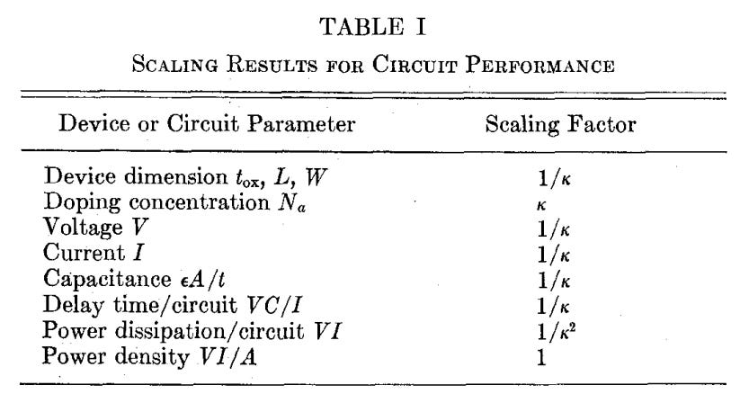
Fig. 14, Source: Ref. CMOS Scaling, 17
The key point in Fig. 14 is that the Power Density is constant as scaling continues.
For capacitance this is driven by the fact that the area reduces as the square (1/k^2), but the distance also reduces by k, so the net result is that the capacitance goes down by k.
Unfortunately, this nice scaling situation is coming to an end*.
*Strictly speaking it already died a long time ago, but the “spirit” of Dennard Scaling (voltage and capacitance reduction) continued long after things like oxide scaling laws stopped.
One key way Dennard Scaling has stopped working is that parasitic capacitances aren’t going down like they used to.

Fig. 15, Source: Ref. CMOS Scaling, 13
The big issue is that parasitic capacitances have gone up, as 3D geometries, shrinking distances and other effects come into play, which has caused the parasitic capacitance’s share of the overall device capacitance to increase (see Fig, 15).
“In many ways, capacitance may represent the most difficult challenge facing the ultimate CMOS device due to the decreasing distances between the gate and other parts of the device (such as the contact and the raised S/D region) and the 1/distance dependence of the parasitic capacitances.”
-Kelin Kuhn, Ref. CMOS Scaling, 12

Fig. 16, Source: Ref. CMOS Scaling, 12
As a result, the capacitance is complex and dependent upon geometry, materials choices, etc. These implementation details at foundries like TSMC are closely guarded secrets. This makes estimating the capacitance from public information challenging.
Nonetheless, we can try and make estimates, and this is fine for directional correctness, and that’s what we’re interested in anyways for estimating the limits.
The “wiggle room” for capacitance is relatively low.
As the distance between two nodes decreases (e.g. spacer capacitance), then the capacitance will go up. This can be reduced with the use of low-k materials, but air is the lowest you can go.

Fig. 17, Source: Ref. CMOS Scaling, 16
Fig. 17 shows an example where a low-K spacer is used, with air gaps possible. This presents mechanical issues, but these may be solvable.
A possibility is that 2-D transistors may allow gate length scaling to continue without experiencing significant short channel effects.
If this were to be the case, the gate capacitance could continue to be decreased. More speculatively, the unique channel control characteristics of 2-D transistors could allow for reducing the parasitic capacitances, but this is speculative.
This gate length would stop at a gate length of ~5 nm, due to direct source-drain tunneling. Although, anisotropic carrier mass engineering may allow a way around this (Ref. CMOS Scaling, 2), but this technique is speculative for now.
Another possibility is to exploit low density of states (DOS) materials such as III-Vs to reduce the effective capacitance on the gate. However, this reduces the drive current (speed) and may cause short channel effect issues.
Vertical FETs can reduce the parasitic capacitances by allowing for density scaling without decreasing the distances between devices as aggressively.
As an example, IBM’s vertical FET paper claims a ~50% capacitance reduction (Ref. CMOS Scaling, 19).
Unfortunately, this is likely a one time boost as well.
Finally, fine-grained 3D integration (e.g. Complementary FETs) can reduce the wire length at the standard cell level, which is often the bigger portion of even standard cell level energy (Ref. CMOS Scaling, 20). But, this is mostly a wire level benefit,
In summary, from first principles, device capacitance is unlikely to drop much below 4X (vertical FETs + 3D), and in fact may go up.
Interconnect Capacitance
Given the situation for device scaling, are wires doing any better?
We will revisit wires in greater detail later on, but for their relevance for capacitance scaling, there isn’t really a good way to reduce wire capacitance beyond ~2X by moving to air gaps.
This is where 3D can have a big effect, potentially greatly reducing the wire length. The third dimension makes wire lengths go from circuitSize ^ (½) to circuitSize ^ (⅓). This is optimistic however, since the number of 3D layers is limited and inter-layer connections are generally more expensive than wires in the same layer.
At the system level, beyond standard cells, 3D integration to reduce wire length could matter a lot, since many (most!) chips are dominated in both power and performance by wires.
Conclusion on Capacitance Scaling
In summary, it’s hard to see more than a ~5X reduction in capacitances, although perhaps a road is possible with 2-D materials.
The IRDS roadmap forecasts an end to capacitance scaling (and power scaling broadly) at around ~2X (Ref. CMOS Scaling, 18), so without a breakthrough of some sort, this is a reasonable practical limit.
Voltage Scaling
Another keystone of Dennard Scaling is reducing the voltage.
Since the energy scales as V^2, this is a powerful lever.
So can voltage scaling continue? Unfortunately things are even grimmer here than in capacitance scaling.
Boltzmann Tyranny
If there is a single takeaway from this article it’s that the Boltzmann Tyranny sets the practical limit because it stops power scaling.
What is the “Boltzmann Tyranny”?
In short, it’s a thermodynamic limit of MOSFETs which limits the “subthreshold swing” to 60 mV/decade.
This means that to increase the current by 10X (a “decade”), you need to increase the gate voltage by 60 mV.
Since you generally need a 10^6 current difference between on and off states for useful circuits, this sets a lower limit of ~360mV.
This can be intuitively understood by taking a source and the drain.
The distribution of the energy levels of carriers on one side is given by the Maxwell-Boltzmann distribution.
An energy barrier (modulated by the gate) blocks these carriers from going to the drain.
Whether the barrier is raised or lowered gives the fundamental switching behavior of a transistor.
If a carrier’s energy exceeds the barrier, then they will cross the barrier to the drain. If not, then it won’t.
Normally, the barrier is high enough to prevent most of the carriers from going over.
However, since the distribution of carriers has a long “tail”, some carriers will have high enough energy to cross the barrier, and this “long tail” means a lot of
Note: technically, the distribution of carrier energies is given by the product of the density of states (DOS) and the Fermi-Dirac distribution, but for the energies we care about this is well approximated by the Maxwell-Boltzmann distribution.
See Fig. 18 and 19:

Fig. 18, Source: Ref. Enhanced CMOS, Energy Filtering, 1

Fig. 19, Source: CMOS Scaling, 21
This sets a fundamental lower limit on CMOS voltage.
And as we saw before, power has a huge impact on the total cost of computing, as well as bottlenecking performance due to cooling limits.
In order to go beyond this, we need a device that operates on different principles, so-called “steep-slope devices”.
We will explore candidates for steep-slope devices in more detail, but for now, no device has high enough speeds (think 10-100X+ slower) to be useful.
Overdrive Voltage
Current processes operate at ~500mV, yet the Boltzmann Limit is ~360mV.

Fig. 20, Ref. Enhanced CMOS, Negative Capacitance
This “overdrive voltage” can be reduced, e.g. with NC-FETs (Ref. Enhanced CMOS, Negative Capacitance, 1), which may allow a ~2X reduction in energy if a Vdd (operating voltage) of ~360mV is achieved in production.
Or, more practically, designers will likely just accept the reduced performance for going to 360mV, which is generally fine as parallel processors tend to be power limited.
Landauer’s Limit
Finally, it’s worth mentioning that there is a fundamental limit to how efficient computing can get based on thermodynamics.
This is called Landauer’s Principle (Ref. Reversible Computing, 4), and sets a lower limit to how efficient computing can get.
This limit is not practically relevant for us now, because we’re still far off from the limits (orders of magnitude) (see Fig. 21 and 22), and run into more near term limits- ie the Boltzmann Tyranny.
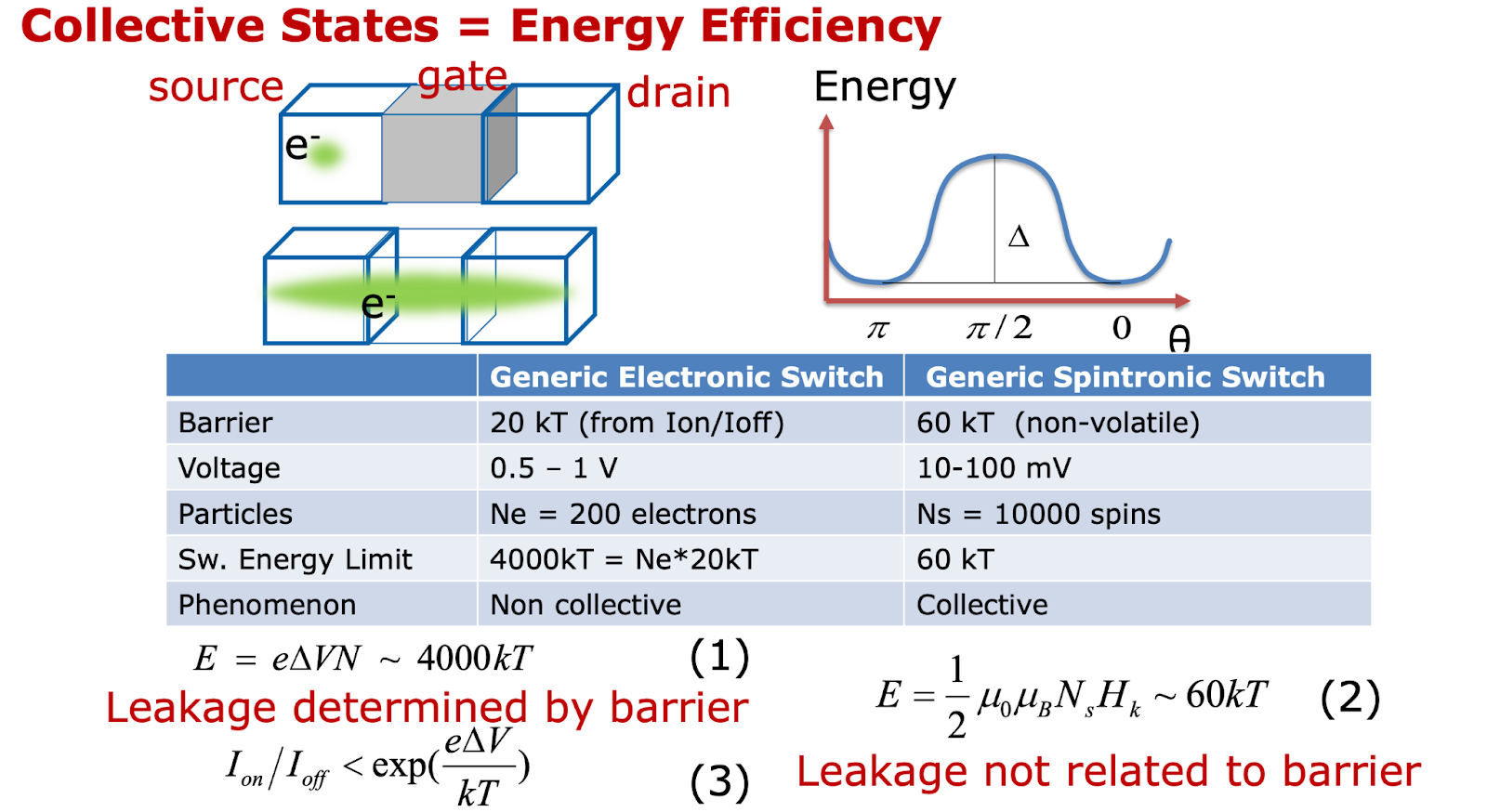
Fig. 21, Source: Ref. Beyond CMOS, 4

Fig. 22, Source: Ref. Reversible Computing, 5
Nonetheless, it is worth mentioning, as it is generally brought up in “limits to computing performance” articles. My article here differs in that I’m interested in how we can practically build computers to get close to those limits.
Reversible computing can get around this, but comes with challenges.
We’ll look at Reversible Computing in more detail later.
Memory
“Compute is free, it’s memory that’s expensive” - Old Proverb

Fig. 23, Source: My own terrible handiwork
As computer architects will know, it’s generally rare that the actual compute (math operations) is the bottleneck, in most real systems we care about, it’s often actually the memory access that is the bottleneck.
This is shown rigorously in the diagram in Fig. 23.
And for some workloads, so-called “memory bound” workloads, this is especially the case.
Memory scaling should be understood (in my view) at three levels:
Cell level
Chip level
System level

Fig. 24, Source: Ref. CMOS Scaling, 22
Since memory is generally organized into arrays, optimizations in shrinking the cell can often be distinct from optimizations done at the array/chip level.
For example, shrinking the dimensions of a memory cell enables higher density, but there are also ways to do this at the full array/chip level.
One such example is given in Fig. 25, utilized in NAND flash, where the peripheral circuitry is implemented in CMOS and put underneath the memory cell array.

Fig. 25, Source: Ref. CMOS Scaling, 23
This distinction is useful for two main reasons:
It shows that even after bitcell scaling has ceased, there still may be density improvements possible
Many interesting parameters such as bandwidth, activation energy and latency are determined at the chip-level and system-level
Memory has historically been determined by minimizing $/bit and increasing density. At the system level it may be more useful to make memory that’s more expensive per bit, but has e.g. lower latency.
Density/Array-Level
SRAM
SRAM scaling is unfortunately another memory technology that has stalled in scaling. SRAM scaling from 5nm to 3nm was effectively zero.

Fig. 26, Source: Ref. CMOS Scaling, 25
SRAM for a long time has used specialized circuit techniques such as read/write assist circuits (e.g. negative bitline and word line boosting) (Ref, CMOS Scaling, 26, 27).
Unfortunately SRAM suffers from both layout related issues as well as high susceptibility to variability. Although threshold voltage variability has been controlled relatively well due to moving from doping to gate work function tuning, SRAM as a circuit is extremely sensitive to Vt variation, making it an issue for SRAM.

Fig. 27, Ref. CMOS Scaling, 27
In addition, there are layout issues that make shrinking the SRAM harder, since the 5nm FinFET layout was very “convenient” for SRAM. Going to 3nm and GAA-FETs means that the layout will be more difficult for at least a generation or two, negating some theoretical density gains.
There are a number of approaches to continue to specifically improve SRAM density however, even if their benefit for logic isn’t as high as it is for SRAM.

Fig. 28, Source: Ref. CMOS Scaling, 28
As an example, vertical FETs could enable denser SRAM by allowing the transistor footprint to shrink without the channel needing to shrink. In addition, Vt variation can be mitigated.
CFETs are another example of this, although the layout is more complicated in this case.
In summary, SRAM density scaling has slowed, and it’s likely that gains will be hard fought from here on out, but not fundamentally constrained.
However, it does seem like SRAM scaling will slow from a practical perspective, and this will pose a challenge for architects. The exact impact of SRAM scaling’s slowdown for each architecture and workload still remains to be seen. And there’s ample room for clever architects to mitigate its impact (e.g. through compression).
DRAM
DRAM, unfortunately, slowed scaling even before logic transistors.
The fundamental issue is that DRAM works by storing states in the charge in the capacitors.

Fig. 29, Source: Ref. CMOS Scaling, 29
So shrinking the DRAM cell size means that the capacitance has to be maintained, but as the DRAM cell size is reduced, the DRAM cell capacitance goes down due to decreased area available.
To compensate, the capacitors can be made taller. But, these capacitors have already been pushed to as high an aspect ratio as reasonably possible, and high-k dielectrics have largely been exhausted.

Fig. 30, Source: Ref. CMOS Scaling, 29

Fig. 32, Source: Memory Scaling is Dead, Long Live Memory Scaling

Fig. 31, Source: SPIE 2021 – Applied Materials – DRAM Scaling - SemiWiki
There are also other issues like charge sharing and interference issues in DRAM cells, but in my opinion, these are less fundamental than the capacitor.
3D DRAM potentially allows for bypassing some limits, since the capacitor is no longer defined lithographically, but by the deposition, potentially increasing the capacitance available.
However, unlike NAND flash, DRAM is already very 3D, since the capacitors are very tall, see Fig. 31.
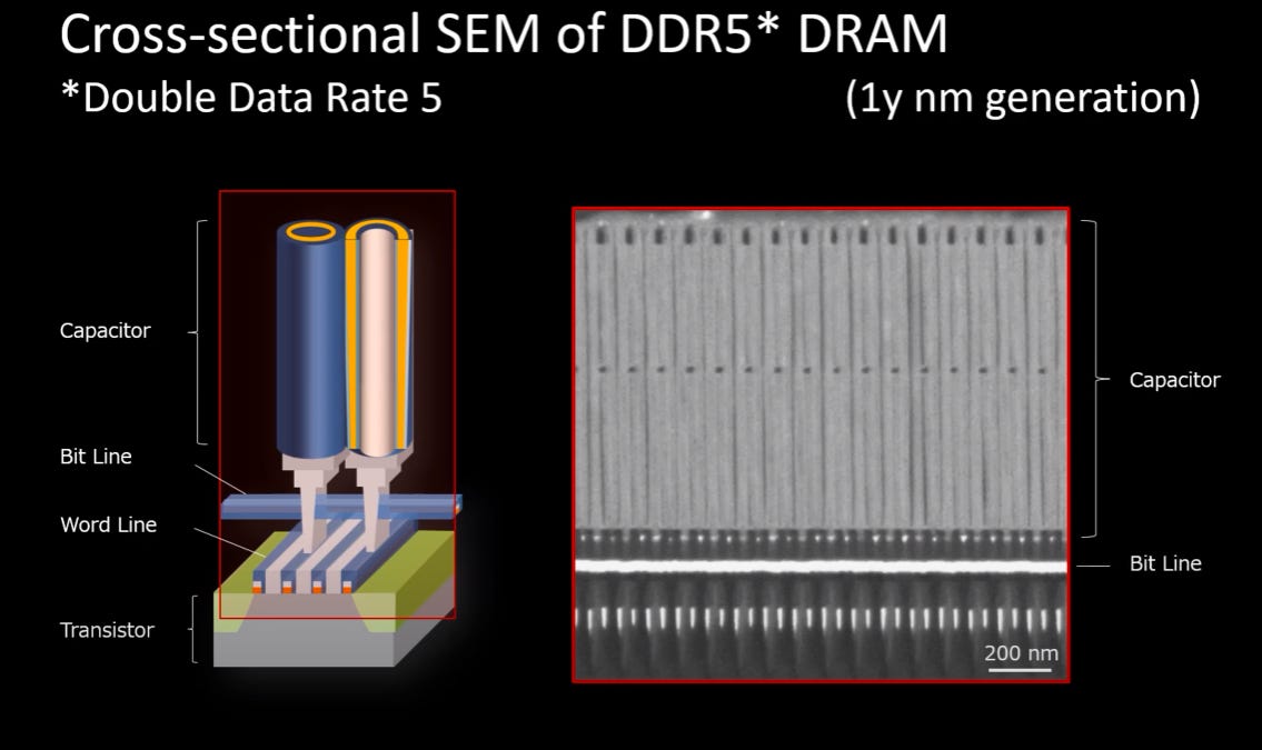
Fig. 32, Source: [Electronics] FIB-SEM tomography of DRAM Memory Cell using orthogonally arranged FIB SEM
As a result, the first 3D DRAMs will have to have a large number of layers to win against this. While not impossible, this is a harder target to hit.

Fig. 33, Source: Flipping cells: 3D monolithic DRAM density increase strategy – Blocks and Files
Finally, going to cryogenic temperatures is an option, as it allows for both scaling the DRAM (leakage gets exponentially better with lower temperature) as well as reducing the latency and energy (lowered resistance in the bit and word lines means reduced time and energy spent in the sense amps) (Ref. CMOS Scaling, 30).
Historically cryogenics has been a non-starter due to the cost and deployment issues. However, as the $ cost of a single DRAM chip continues to go up (due to increased processing costs), it may start to make sense to use cryogenics to bring down the total $/bit.
DRAM dies also generally have lower power density compared to logic, making the cost of cryogenic cooling much lower.
In addition, DRAM modules have historically been used in laptops and desktops, where cryogenic cooling is infeasible. If workloads primarily migrate to datacenters, this may not be an issue anymore.
There may also be system level benefits. Eg the latency can be 2x or lower for cryogenic DRAM. For latency bound workloads, e.g. single-threaded CPUs, this could be very valuable, extending beyond the cost benefits at the DRAM level, and rather to performance benefits at the workload level.
Emerging Memories
Okay, given the grim, but not hopeless situation for DRAM, what about alternatives? Unfortunately, most of the alternatives to DRAM are orders of magnitude off in the key parameters.
Historically the computer architecture community has viewed alternatives to DRAM, such as phase change memory or ReRAM as taking the place in the memory hierarchy between DRAM and storage.
Fig. 34, Source: When memory and storage converge - Rambus
However, this largely proved to be less useful than hoped.
Instead, we will look at memories that can potentially replace DRAM or SRAM.
FeRAM
FeRAM, or ferroelectric RAM, relies upon using the polarization of a ferroelectric material to store the state.

Fig. 35, Source: Ref. CMOS Scaling, 31
It’s interesting since it can have very high density and is nonvolatile. Given the slowdown in SRAM scaling, this is being investigated for both replacing DRAM as well as replacing SRAM. Given that it is less sensitive to thermals compared to DRAM, FeRAM might very well be a viable technology to replace SRAM for some applications.
Traditionally FeRAM would’ve been a non-starter in CPU applications due to much higher latency (2ns+ generally), but for AI and other parallel applications with large working sets, this might be just fine.
FeRAM and its cousins appear to be promising, and the high cost can likely be brought down over time, and may indeed be irrelevant if it is integrated onto logic chips and competes with SRAM instead of DRAM.
ReRAMs
ReRAMs are broadly a class of memories that rely upon a mechanism to switch the resistance level between two electrodes. There are many ways to achieve this, from ion migration to metal-insulator transitions and even carbon nanotube switching.
Since ReRAMs generally have endurance far below what is needed for compute-level applications (10^12 for ReRAM vs 10^15 for DRAM), are much slower (10-100X+ slower), and have higher voltages, they’re generally not suitable for compute applications, so we’ll avoid going into much detail on them.
MRAM
Two major types: STT-MRAM and SOT-MRAM.
These suffer from the same set of issues as ReRAM, although highly scaled SOT-MRAM may allow for SRAM-like operation, especially for higher levels of the on-chip memory hierarchy (CMOS Scaling, 34).
Unfortunately, SOT-MRAM cell size is surprisingly large, which often makes it much less attractive against SRAM:

High density SOT-MRAM memory array based on a single transistor

A Recent Progress of Spintronics Devices for Integrated Circuit Applications
On the bright side, SRAM isn’t scaling, but SOT-MRAM might, which could still be useful!
System Level
System level parameters such as bandwidth and energy are often set by the system level aspects, principally, the packaging.
Latency in DRAM is generally set by the array level characteristics instead of the packaging however.
Bandwidth
Memory bandwidth is generally something set by the packaging technology, not the cell/array level technology.
On-chip memory (i.e. caches and scratchpads) generally have incredibly high BW, but are far too small for most interesting workloads to fit into.
The wires between the chip and the DRAM module are generally the limiting factor for DRAM bandwidth. The move to HBM (high bandwidth memory) has greatly increased BW, but for some workloads more is needed.
HBM BW can likely be pushed much further with no fundamental limits, especially since signaling rates over the substrate can be dramatically increased.
However, at some point power starts to become the limiter, as high end HBM stacks are already at ~25W each.
To push to even higher BWs and lower power, 3D stacking of DRAM on top of logic is the way to go.
This however is extremely challenging since increased heat exponentially increases DRAM’s leakage and therefore refresh rate (reduced retention). There is also the possibility of reliability issues since mechanical and interference issues could be worsened.
Nonetheless, these issues aren’t fundamental, and novel engineering concepts, e.g. microfluidics or spray cooling could solve them.
Another possibility would be to use lower power computing technologies with lower speed, e.g. low-voltage CMOS, TFETs or reversible computing which would allow the DRAM to be 3D stacked without the thermal constraints becoming overwhelming.
In summary, there seem to be valid routes to increasing DRAM bandwidth significantly in the years to come.
Latency
The latency of DRAM is set by the time spent in the sense amplifiers, not because “it is further away” like is normally claimed. Moving the DRAM closer to the chip (or even on-chip) would barely make latency budge,
Reducing the number of DRAM cells in a row would reduce the latency, but would subsequently make density go down and thus $/bit go up.
This is the reason why historically this approach has been taken.

Fig. 32, Source: Ref. CMOS Scaling, 32

Fig. 33, Source: Ref. CMOS Scaling, 32
An approach called “Tiered Latency DRAM” however, could allow the DRAM latency to be brought down, while still remaining economical.
Finally, with the rise of memory disaggregation (e.g. CXL), DRAM utilization may go up significantly, potentially allowing for DRAM utilization to go up, and only for programs that need the low latency DRAM to be used. This may make low latency, high cost DRAM economical, and potentially in a mixed capacity,
In conclusion, DRAM latency is not as easily improvable as bandwidth, but there are viable routes to improving it moderately (especially if cost increases can be tolerated), which for memory latency bound applications could be very useful for performance.
Energy Access of Memory
Many systems are also bound by the energy cost of accessing DRAM (especially bandwidth bound applications). How much can energy be reduced?
In this case the primary contributor is the energy spent in moving the data around.
Given this, it’s reasonable to expect advanced packaging technologies like HBM or 3D stacked DRAM to reduce energy costs.
Conclusion on Memory
In summary, we can see that bitcell level scaling for both DRAM and SRAM is slowing, with few contenders able to take their place. Although scaling will continue, gains will be hard fought from here, and it’s hard to see a gain more than ~10X.
However, the bright side is that significant improvements in bandwidth and energy are possible and practical. Latency can also likely be improved, but not quite as much.
Finally, ferroelectric memories offer a potential bright spot in the landscape of scaling options.
Wires
“Transistors are free, it’s wires that are expensive”- a wise man.
Arguably transistors are not the bottleneck for most chips, wires are.
This is both from a performance standpoint and an energy standpoint (in fact, even in some standard cells the wire consumes the dominant share of energy!).

Fig. 34, Source: Main, 21
And worse, wires, unlike transistors, do not get better as they scale down.
When a wire is scaled down, the resistance goes up, and the capacitance stays the same (due to the distance between two wires going down, even as the area goes down).
So wires actually get worse as they get smaller! And with the end of voltage scaling, energy isn’t going to get lower either, even as transistors get smaller. So are we screwed?
Well, not quite. There are, broadly speaking, wo types of wires:
local and global wires
Local wires, e.g. wires in a gate between transistors and wires between gates do get “better” since they get shorter. As gates become smaller, the distance between them decreases, and the wires become shorter.

Fig. 35, Source: Ref. CMOS Scaling, 24

Fig 36, Source: Ref. CMOS Scaling, 24
It’s also worth noting that the shift to tiled manycore architectures like AI chips has made some “global wires” scale down
In these chips the number of cores is generally increased instead of increasing the transistor count of each core (e.g. 100 to 200 cores). This means that a “global” wire in the NoC that connects two cores shrinks down in length.
That is “scaling as usual”. Unfortunately, scaling as usual is no longer valid, and the resistivity of wires is increasing at a faster rate than what would normally be the case.
This is driven by two primary factors:
Copper grains and linewidths becoming small enough that the electron mean free path is larger in comparison
Leading to scattering
Linewidths are becoming small enough that the high resistance barrier material is becoming a larger proportion of the total wire volume
The previously negligible area (and therefore resistance) of the barrier is now no longer negligible

Fig. 37, Source: Ref. CMOS Scaling, 33

Fig. 38, Source: Ref. CMOS Scaling, 33
Fortunately, there are options around these issues. One option is to use single-crystal metals without grain boundaries in them (there is speculation this may be in research at TSMC). Another is to move to another material whose EMFP (electron mean free path) is lower.

Fig. 39, Source: Ref. CMOS Scaling, 33
Both of these paths are likely to be pursued by the chip industry, and it seems that the issues with increased resistance at lower linewidths aren’t fundamental.
Similarly, as long as transistor sizes continue to scale down, the length of wires will continue to go down as well, to a first order maintaining their relative contribution to the energy and delay of circuits.
Finally, using the backside of the chip for additional wiring (“active backside”) could allow for reduced routing congestion and reducing capacitance by increasing the spacing between wires.
Optical Wires
It’s worth mentioning the promise and perils of a different paradigm for interconnects: optical “wires”.
Due to the size limits imposed by the wavelength of light and the coupling between adjacent waveguides, optical waveguides are limited to 500 nm-5um in pitch. This is, of course, far too big for local wires that connect transistors and gates together (~20-50 nm width, M0-M4), but could potentially replace global wires that connect blocks together.
On-chip optical networks, often called “optical network-on-chips” or “nanophotonic network-on-chips” have been proposed to alleviate the issue of global wires.
For workloads in which there is low (or no) locality, this would be a godsend, since it would theoretically allow accessing any part of the die at the same energy and (approximately) latency cost.
This is because of the common knowledge that “electrical <> optical conversion is expensive, but once you’re in the optical domain, more distance doesn’t consume more energy”.
Unfortunately, this common knowledge is not really accurate. The offending factor is the loss of waveguides. The issue is that on-chip waveguides are lossy and have propagation losses measured in dB/cm.
When this is compared to the energy levels that low-swing electrical interconnects can achieve, the situation becomes less of an obvious win.
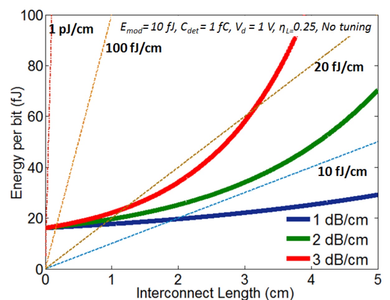
Fig. 40, Source: Ref. Main, 10
As can be seen from Fig. 40, at a high enough propagation loss (1-3 dB/cm is a reasonable range), the losses start to increase exponentially at surprisingly small distances, and drive energy costs up.
Fortunately, these issues are not insurmountable, and other materials platforms such as SiN or low-contrast SOI can reduce propagation losses significantly (see Fig. 41).
Fig. 41, Source: Ref. Main, 11
The best electrical interconnects achieve energy of about 10 fJ/bit/mm*, against which an idealized optical link is competitive, and with lower losses, better.
*This requires ~2um wires, to have low resistance, but since optical waveguide spacing is ~5 um to avoid crosstalk issues, this is comparable.
Nonetheless, the cost of optical on-chip interconnects is currently prohibitive, and so far the number of applications that are a “killer app” for it appear limited (i.e. lower energy, lower latency and higher BW).
In summary, optical interconnects are likely viable in their role of potentially replacing global wires, but would require considerable improvements in cost and economies of scale to practically achieve.
Economics
Cost (how much lower can it go?)
How much cheaper can we make chips?
This is relevant to approaches like reversible computing or low voltage CMOS that attempt to trade off compute speed for energy efficiency.
The long story short is that chips can get cheaper, but huge reductions are limited by the fact that there are many contributing factors to the cost of a chip.
Although lithography and etch dominate, if a >10x reduction in cost is desired, then even things like the cost of the actual silicon wafer become an issue. Although there are potentially ways around this (e.g. thinning the wafer via ion implantation and cleave), it goes to show that there are many blockers to expecting eg a 32x reduction in cost that would enable a 32-layer 3D chip to be the same cost as a normal 2D chip.

Fig. 42, Source: Ref. Economics, Economics of 3D, 4
Although the breakdown in Fig. 42 is fudged, it goes to show that even if lithography and etch costs were to be reduced to zero, other costs would still prevent a >5x reduction in the cost of the chip.
3D NAND Flash Economics
One interesting possibility for scaling into 3D without the cost of the chip going through the roof is to use a design where the

Fig. 43, Source: Ref. Economics, Economics of 3D, 5
Currently, there’s not a known method for how to do this logic, due to the irregularity of logic design and the fact that there’s a very specific design with 3D NAND that allows this to work.
Nonetheless, there may be a way to make this work, especially with approaches like 3D self-assembly.
Beyond the Known Transistor
So silicon MOSFETs have fundamental issues with energy reductions set by the Boltzmann tyranny.
What about going beyond that?
What about replacing silicon as the material?
What about breaking out of CMOS as a paradigm, maybe even beyond electrical charge as the computing mechanism?We’ll explore these, and other ways to go “beyond the known transistor”:
Benchmarking

Fig. 44, Source: Ref. Beyond CMOS, 5
First, before diving into detail, let’s look at an overview of various device types. Our goal is to say, if CMOS weren’t the established technology, and we were given the full spectrum of choices to pick, what would we pick?
Fig. 44, from a benchmarking study done at Intel, gives a snapshot overview of a wide variety of devices. Although it’s not exhaustive, it does give a good overview. The long story short is that it’s not looking good. Very few devices beat CMOS in the energy-delay tradeoff curve.
Even those that do, don’t beat it by a big margin.
The good news is that since the bottleneck is power, and not performance, this relaxes the target- devices which have worse EDP but have lower E (energy), are still viable.
Unfortunately, even when looking at devices with lower energy only, the list of candidates is limited.
“Enhanced CMOS”
I’ve broadly attempted to categorize beyond-CMOS devices into “Enhanced CMOS”, which is a loose term for device structures which resemble CMOS transistors, and “Beyond-CMOS”, a loose characterization of the more exotic options, which depart from the MOSFET structure, such as spintronics.
Negative Capacitance FETs
The fundamental issue posed by the Boltzmann Tyranny is that a certain voltage is needed to raise or lower the energy barrier in a transistor channel.
Two capacitors in series cause the voltage to be divided, but what if there was a negative capacitance, then the voltage would be amplified. How can we get such a negative capacitance?
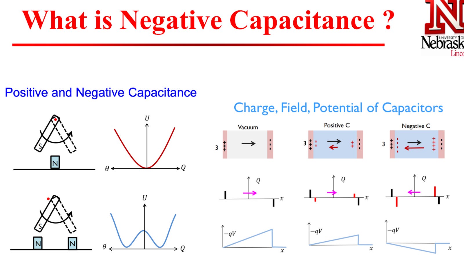
Fig. 45, Source: Ref. Enhanced CMOS, Negative Capacitance, 2
Such a negative capacitance can be realized through the use of ferroelectric materials, which have two stable states of electrical polarization. In the process of switching from one state to another, a transient “negative capacitance” effect can be realized.
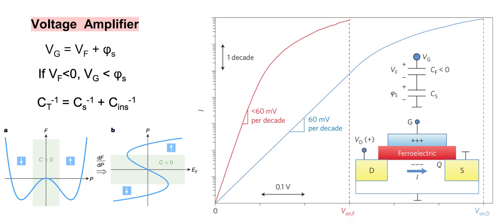
Fig. 46, Source: Ref. Enhanced CMOS, Negative Capacitance, 2
In theory, this should then allow for the effective voltage needed to switch a transistor to be reduced.
However, there are problems.
First, is the problem of metastability. This issue was hoped to be overcome with stabilization when in series with a normal capacitor.
Second, is the issue of hysteresis. The ferroelectric material essentially has two stable low energy states, with only the transient center exhibiting the negative capacitance. This ordinarily creates hysteresis (fig. 47) , which makes it unusable for logic. Simultaneously having hysteresis-free operation and low subthreshold swing remains an open question.

Fig. 47. Source: Ref. Enhanced CMOS, Negative Capacitance, 3
There are also questions as to the experimental validity of the voltage amplification effect.
Unfortunately, so far there has not been good experimental evidence of hysteresis-free sub-60 mV/decade FETs. (Ref. Enhanced CMOS, Negative Capacitance, 1).
Whether this is because of fundamental issues with negative capacitance FETs or due to engineering/research issues is still an open question.
There are also concerns around the speed of switching for negative capacitance devices. Most negative capacitance effects rely upon switching between states in a ferroelectric, but this usually involves ion transport or some other slow mechanism, which is slow. Globalfoundries demonstrated devices based on electron cloud switching, but even this is slower than current CMOS devices.
(Ref. Enhanced CMOS, Negative Capacitance, 4)
Negative capacitance devices are very alluring- take a normal transistor, add some negative capacitance and the energy goes down!
Unfortunately, currently both the experimental and theoretical evidence is limited. For now, negative capacitance devices
Breakthroughs here would change the trajectory of computing significantly.
Tunneling FETs
Tunnel FETs work by changing the fundamental mechanism of transistor operation. MOSFETs work based on the principle of thermionic emission, as the potential barrier in the channel is lowered, carriers with a high enough energy can diffuse across the channel from source to drain. However, as we saw before, thermionic emission requires an energy distribution with a long tail (Fermi-Dirac, or approximated as a Maxwell-Boltzmann distribution). However, since tunneling FETs don’t

Fig. 48. Source: Ref. Enhanced CMOS, Tunneling FETs, 1
Unfortunately, tunneling FETs have very low on-state currents, which has essentially made them a nonstarter for CPUs. Even for parallel workloads like AI, this isn’t economically viable.
To put this into perspective, the best experimental results for TFETs for sub-60 mV/decade swing are ~1 uA/um, while CMOS is ~500 uA/um (Ref. Enhanced CMOS, Tunneling FETs, 2)- this is 500X slower!
This is a complete non-starter for most applications.
There may however be use cases for TFETs in very power limited applications where performance isn’t important, but battery life is at a high premium. This may especially be the case when high performance is required for only a short period, and most of the time is spent in a background/standby mode. Examples could include mobile uses like smartphones, smartwatches, and even sensor nodes.
Simulations with TFETs have shown much better results, but the issue is a significant mismatch between simulations and experiments.
This makes it both a) hard to trust predictions with TFETs, due to our poor understanding of them and b) progress unpredictable in them.
(Ref. Enhanced CMOS, Tunneling FETs, 1)
One nice thing about TFETs is that due to their different mechanism of operation, they are generally not impacted by the same short-channel effects that cause MOSFETs to get worse as they scale down.
In conclusion, TFETs have no fundamental flaws (that we know of), which makes them a promising direction for research, but are currently very far off the target of being anywhere near viable.
Cold Source FETs
These devices work by filtering out the long tail of high energy carriers with narrow bandwidth semiconductors- hence “cold source”.

Fig. 49, Source: Ref. Enhanced CMOS, Energy Filtering, 1
Like TFETs, they suffer from very low drive currents, and like TFETs, are also reliant upon DFT (density functional theory) for predictions,
Unlike TFETs, they are a relatively immature technology and their parameters are currently much worse than TFETs, which themselves are much slower than MOSFETs.
Non-Silicon CMOS
Okay, so we’ve discussed the challenges with silicon CMOS- can we do any better with moving beyond silicon? After all, we’ve heard some variant of “Silicon Valley will be called Graphene Valley” for a decade now- maybe that time has come?
Can This Even Help?
It’s important to note that a MOSFET made of a different channel material than silicon is still a MOSFET! It cannot break the Boltzmann tyranny, so voltage scaling is not possible (except for overdrive voltage reduction).
However, some of these materials may allow for capacitance scaling, e.g. increased drive strength could allow for reduced transistor width, and/or reducing the “track height’ of a standard cell.
In addition, these materials allow for improved carrier mobility even as the size shrinks, and improved control over the channel, even as the gate length shrinks.
These characteristics have made these non-silicon materials attractive for foundries to explore for future process node generations (eg for TSMC).

FIg. 50, Source: Ref. Enhanced CMOS, Carbon Nanotubes, 1.
Eg in the figure above, we see that using carbon nanotube transistors (CNT-FETs), a 4x smaller effective width is needed to achieve the same drive current. This would allow for narrower transistors while maintaining speed, or depopulating the “track height” in a standard cell.
Unfortunately, “track height” reduction has already been aggressively pursued, and with 5 track cells expected to be used by 2nm, this lever may soon be out of steam.
Another avenue is decreased channel volume, which may decrease the parasitic capacitances. A 2-D TMD or CNT channel would have a much smaller channel volume than silicon for the same drive current.
Finally, reducing the parasitic capacitances of more complicated mechanisms, e.g. the parasitic capacitance of the punch-through stop layer, may be possible, but this is hard to analytically capture.
Many papers argue that there is an “EDP” (energy delay product) advantage with a new transistor platform. Traditionally, the EDP metric has been the dominant metric, since it accurately captures the tradeoff frontier between power and performance.
Looking at EDP, it would appear that these new non-Si devices are in fact a significant improvement!
Unfortunately, in the power limited regime (true both economically and cooling wise today), the delay part of EDP is less important than the energy part. When the EDP benefit is decomposed into energy and delay, it can be seen that all of the benefit is in the delay component, with energy not going down at all (in most cases).

Fig. 51, Source: Ref. Enhanced CMOS, Carbon Nanotubes, 2
For example, we can see here that even though there is a large reported EDP benefit against silicon devices, the operating voltage is the same for almost all the devices.
That same paper argues that CNT-FETs have 30% lower capacitance compared to Silicon GAA-FETs however, which shows that there could still be capacitance gains (and therefore power gains) from going to non-silicon channels.
III-Vs
III-V compound semiconductors have been explored for decades, since the first silicon circuits were built. The promise over the decades has been higher carrier mobility, enabling faster operating speeds.
Many of the historical roadblocks (e.g. lack of a native oxide like silicon dioxide), more expensive wafers, etc) are largely no longer issues.
(HKMG doesn’t use a native oxide anyway, and wafer costs are dwarfed by ~100X by processing costs)
Unfortunately, III-Vs today, at nanoscale suffer from direct source to drain tunneling issues.

Fig. 52, Source: Ref. CMOS Scaling, 13
III-V materials also have a reduced quantum capacitance due to reduced density of states (Ref. Enhanced CMOS, III-Vs, 1, 2, 3).
This effect reduces the drive current, but may be exploitable to reduce the capacitance, and thus, power.
However, this does reduce the drive current of the transistor, and therefore its speed. For CPU applications, this is likely a non-starter, but for parallel computing applications (eg AI), this may be worthwhile.
Note however, that this doesn’t reduce parasitic capacitance, and therefore, may prove to not be worthwhile once this is considered.
As we saw before, transistor parasitics are starting to dominate the total capacitance.
Finally, since nanoscale transistors operate in a quasi-ballistic regime, increased carrier mobility is not as directly relevant as is the diffusive regime.
In summary, III-Vs seem like a technology whose window of opportunity has sadly passed, and with no benefit for the fundamental problem of the Boltzmann Tyranny for power scaling.
Two possible use cases for III-Vs however are for TFETs (heterojunction TFETs have higher drive current), and for photonics (III-V devices offer superior active components and lasers than silicon).
2-D TMDs
2-D TMDs have been the subject of intensive research among the major foundries for a while now. They offer a number of useful advantages for making smaller transistors:
Good carrier mobility, as the channel scales down
As silicon scales down in channel thickness, the mobility very quickly drops
This is a problem since the channel needs to be scaled thinner to avoid short channel effects as the transistor gets smaller (even with GAA-FETs).
Control over the channel
Because the channel is so thin, excellent control over the channel is possible, giving excellent electrostatics, see Fig. 52.

Fig. 52, Source: Ref. Enhanced CMOS, 2-D TMDs, 5
They also bring a number of challenges:
Challenges of contact formation
Forming low resistance contacts between metals and 2-D TMDs is challenging
Wafer-scale growth with high yield
Growing these materials without prohibitively high defectivity at the wafer level is still challenging
These advantages are very useful for continued scaling of transistors in terms of density, but they do nothing about the energy problem.
The reduced channel volume of the 2-D TMDs will likely reduce the capacitance to some extent, but should be a one-time benefit.
The other issue is that 2-D TMDs essentially mean forfeiting the use of vertical FETs, which removes one powerful axis for reducing parasitics, and therefore power.
To conclude, 2-D TMDs will likely be the material of the future in terms of how scaling is currently being pursued, and also being favored in pathfinding groups at major foundries (ie Intel and TSMC), but don’t address the key problem of power and the Boltzmann Limit.
Carbon Nanotubes
Carbon nanotubes essentially have the same set of issues as 2-D TMDs, with a few additional issues around metallic CNTs that further impact yields. They do have even higher carrier mobility and therefore drive current, which allows even greater reduction of the channel volume.
However, the same set of tradeoffs and challenges exists as with 2-D TMDs (just to a greater extreme), so we’ll avoid spending much time on them.
Beyond CMOS
Finally, the big prize- replacing the transistor!
A wide variety of devices can be called “Beyond CMOS”, and most of them suck!
Broadly speaking, there needs to be a physical mechanism for:
Switching
How the on/off is done
Eg spin-orbit
State variable
How are 1s and 0s represented?
Eg charge or spin states?

Fig. 53, Ref. Beyond CMOS, 2

Fig. 54, Ref. Beyond CMOS, 6
Fig. 55, Ref. Beyond CMOS, 2
There are many, many combinations of these, so Nikonov’s group and the “The Future Transistor” paper have put together a taxonomy of them (Fig, 53, 54, 55).
Spintronics
Spintronics refers broadly to a group of devices that utilize spin and collective states as the computational state variables.

Fig. 56, Source: Ref. Beyond CMOS, Spintronics, 1
As Fig. 56 shows, there are a wide variety of spintronic devices, far outside the scope of this article to cover.
So, we will rely upon benchmarking:
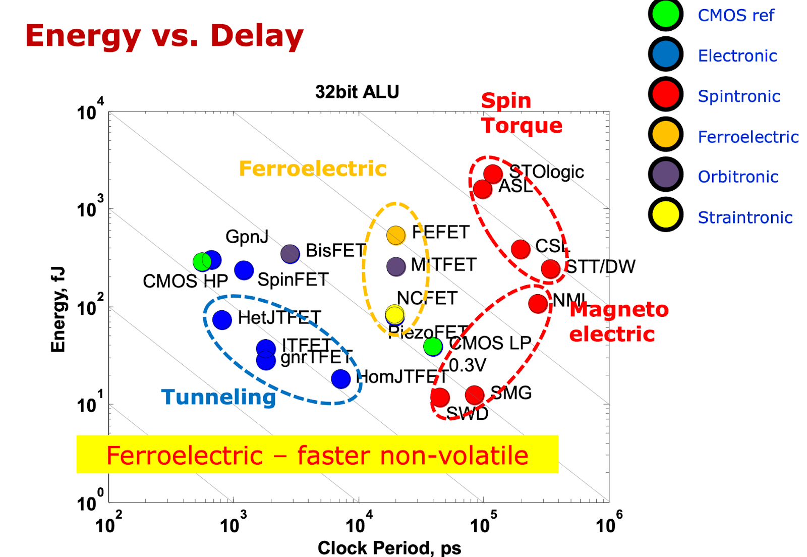
Fig. 57, Source: Ref. Beyond CMOS, Spintronics, 1
As can be seen from Fig. 57, all currently benchmarked spintronic devices are orders of magnitude worse in EDP than CMOS references.
The EDP is worse, but what about just the energy? The issue with this is that even though there are spintronic devices with lower energy (e.g. SMG and SWD), the delay is orders of magnitude worse, a factor of 100X.
In these cases, the tradeoff is not worth it. Even for the most energy efficiency sensitive applications, e.g. bitcoin mining, the rule of thumb ratio is generally 10:1 in the ratio of power cost to chip capex.
In conclusion, spintronics devices hold some promise for very low power applications, but in general are currently too slow for most use cases.
MESO
A notable exception to this grim outlook for spintronics is the MESO device (short for “magnetoelectric spin orbit”).
Essentially, this works by taking charge as input, using that charge to switch a magnet with a capacitor (magnetoelectric effect), computing in the spin domain, then taking the spin and convertering it back out to charge (spin to charge conversion).
Input (stateVariable = electric charge) →
switching mechanism (magnetoelectric effect) →
internal state (stateVariable: spin state) →
outputTransducer (spin to change conversion) →
Output (stateVariable = electric charge)

Fig. 58, Source: Ref. Beyond CMOS, Spintronics, 2
Using the classification of Fig. 55, the input state is charge, the internal state is magnetization, and the output state is charge.

Fig. 59, Source: Ref. Beyond CMOS, Spintronics, 2
The MESO device uses the magnetoelectric effect, which is more efficient than current controlled magnetic switching, and through the spin to charge conversion effect, eliminates the need for a “transducer”, allowing the inputs and outputs to both be charge, which further increases efficiency.

Fig. 60, Source: Ref. Beyond CMOS, Spintronics, 2
This enables MESO to be an extremely efficient logic device, and has other advantages as well (which we’ll discuss in the next section).
As seen in Fig. 60, MESO is able to match the pareto frontier in EDP for the best CMOS and beyond-CMOS devices, while also offering a low energy/op that CMOS (or any other beyond-CMOS device) cannot.
Even better, MESO gets more efficient as it scales down, in contrast to MOSFETs, which get worse (short channel effects), as they become smaller.
Today, there is no material system at room temperature that achieves the required magnetoelectric coefficients and spin-to-charge conversion efficiency. However, a working MESO device has been demonstrated at room temperature (Ref. Beyond CMOS, Spintronics, 3). Currently the output voltage is orders of magnitude below what’s needed, but it provides a baseline to build off of.
In summary, MESO is an extremely promising device technology, and breakthroughs in it could change the trajectory of Moore’s Law, and the conclusions of this article!
Majority Gates and Non-Volatility
Spintronic devices have some other advantages, which are not directly reflected in simple energy, delay and area numbers:
Non-volatility
Eliminates pipeline register energy
Majority gates
More compact, and energy efficient for multipliers and adders
Non-volatility of logic allows for eliminating pipeline register energy, which has two benefits:
Reduces energy
And glitch energy
Allows for increasing pipeline depth, and thus clock speeds, without increasing pipeline register energy
AI chips have no branches, so can crank up speeds to 10GHz+ !
Potentially also useful for reversible computing

Fig. 61, Source: Ref. Chip Level, AI Chips, 2
In many cases, the pipeline register energy can be significant, see eg Fig. 61. Eliminating this energy allows for increasing pipeline depth, and offsetting many of the slow operating speed downsides of spintronic logic.
It also allows for interesting tradeoffs, since you can potentially use systolic arrays, or other microarchitectures, which might be more energy efficient (e.g. higher data reuse than wide-vector tensor cores) when pipeline register energy is eliminated.

Fig. 62, Source: Ref. Beyond CMOS, Spintronics, 2
Spintronics devices, by nature of their collective based state, allow for efficient majority logic gates.
This enables more compact implementations of arithmetic circuits, especially multipliers and adders (3 gates vs 28 transistors).
This alone gives a big boost for e.g. AI chips or bitcoin mining chips, where the majority of the logic is adder or MAC circuits. (For bitcoin mining in particular, the nonvolatile nature allows for reducing the energy of the pipeline registers in the input to the SHA-256 round block)
But, for certain systems, e.g. AI chips, there are potentially additional second-order effects. In many AI chips, the majority of the energy is dissipated in the wires between circuit blocks. More compact datapaths from spintronic devices could allow for reducing this, giving energy efficiency gains beyond what would be expected by simply swapping in the MESO energy value for the datapath energy.
These two cases both highlight the need for system level evaluation for process technology pathfinding, to capture these higher order effects. Simple circuit or device level EDPs will no longer suffice in the modern era of computing!
Estimation approaches like Neurometer (NeuroMeter: An Integrated Power, Area, and Timing Modeling Framework for Machine Learning Accelerators) are one way to approach this.
NEMS/Straintronics
NEMS devices utilize nanoscale mechanical movement to achieve switching, kind of like a nanoscale light switch.
NEMS devices can often have very low power, beating CMOS energy efficiency, at the cost of delay. Generally, the tradeoff is around 10X slower speeds and 10X lower energy. Unfortunately, NEMS devices are generally gigantic in area compared to CMOS devices, which makes them nonstarters.
“Our simulations suggest that the proposed short-circuit current free NEMFET gates exhibit up to 10x dynamic energy reduction and up to 2 orders of magnitude less leakage, at the expense of 10 to 20x slower operation, when compared with CMOS counterparts.”
- Ref. Beyond CMOS, NEMS, 2
Straintronic devices (e.g. piezoelectric devices) offer the opportunity to be smaller and faster, but lack good experimental data (Ref. Beyond CMOS, NEMS, 1).
Switching endurance and reliability are also major unknowns here, since 10^17+ cycles are generally required for logic applications.
There are also concerns about stiction as a function of scaling down in dimensions.
In conclusion, breakthroughs here could be revolutionary, but there are many challenges, such as experimental evidence, reliability and size.
Mott FETs
Mott FETs utilize the metal insulator transition to achieve incredibly high switching speeds and low subthreshold slopes.
Unfortunately, these require very high voltages to achieve these effects, negating their benefits. If negative capacitance effects end up working, this could be an interesting angle to pursue.
“Throughput-Volume” Paradigm
A number of approaches with reduced speed or density per unit area plan to go into 3D in order to recover performance (for parallel workloads), and rely upon the cost of 3D transistors falling compared to 2D transistors. Or more generally on transistor cost being scaled down, allowing a tradeoff between energy and transistor usage.
Examples include reversible computing, superconducting logic, TFETs, etc.

Fig. 63, Ref. Reversible Computing, 3

Fig. 64, Ref. Reversible Computing, 3
Unfortunately, the number of layers required for this approach is generally prohibitive from two perspectives:
Economics
Cooling
First, as shown before, the transistor cost reduction generally comes from packing more devices onto a wafer or layer, there is no single clear lever (even if lithography is dominant) that allows for massive cost reductions. Adding more layers adds more cost.
Second, even if the total energy dissipation is constant, adding multiple layers of chips (especially very high numbers like 1000+), means that cooling the middle parts of the chip stack is very challenging, as the heatsink is far away, and heat has to travel through many chip layers.
Source: My talk from a long time ago
Thinning each chip/layer helps, but thin materials have poorer thermal conductivity properties.
In addition, the inter-layer resistance (die to die resistance), is often the primary driver of thermal resistance, which gets much worse with many layers, see Fig. 65.

Fig. 65, Xylem: Enhancing Vertical Thermal Conduction in 3D Processor-Memory Stacks
In conclusion, with current known manufacturing techniques and thermal issues, there isn’t a practical path to using many layers in 3D to economically trade off reduced compute per transistor for reduced energy per computation to an arbitrary degree.
This tradeoff of reduced energy for reduced compute is a good idea, but not to an arbitrary extent.
Chip Level
So far we’ve focused on the gate-level, what about at the level of the entire chip?
The Opportunity
Fundamentally, the possibility at the chip level boils down to two things:
Wires
Memory
Which in some ways is just about wires
In a way, the problem of wires has been with us since the very first days of microelectronics. Noyce’s integrated circuit was such a breakthrough because of how it elegantly integrated wires, much better than Kilby’s IC.
As shown above, the energy spent in wires can be significant even between logic gates, and between blocks in a chip, a huge amount!
Wires also add significant latency, which for some workloads, e.g. in CPUs, can be the far bigger factor (compared to transistor scaling).
Fig. 66, Source: Ref. Chip-Level, AI Chips, 1
Take for instance an AI processor for a computationally intensive workload. Fig. shows the energy breakdown for MAGNet, a CNN accelerator. Although CNNs are now ancient history, the paper still acts as a representation of the energy breakdown for a computationally intensive workload. (Also, workloads like diffusion models still use CNNs)
Even for this computationally bound workload, most of the energy is not spent in the datapath- but rather in registers and buffers of some sort!
Memory access energy roughly scales as the square root of the size of the memory array (the wires in the memory array primarily), so reducing the size of the memory array is a big energy win.
So what can be done to improve upon this huge source of energy consumption?
New Memory Technologies
We’ve already covered the wide array of potential options. These options could reduce the area taken by memory, and thus greatly reduce the on-chip wire energy. This would be the case both for larger memory arrays (scratchpads and caches), but also for smaller memory arrays (register files).
One thing worth mentioning is that eDRAMs with small capacitors (gain cells, in the extreme, with no explicit capacitor) can be useful for some ML workloads, since many operand values are stored for less than 10 microseconds (eg a lower level register file in an HRF for a GEMM).
3D Chips
Folding a 2D chip into 3D would greatly reduce the wire length, both between blocks and inside memory arrays.
This would save a large amount of energy in wires.
There are two primary levels this can happen:
Coarse grained
Fine-grained
In the coarse-grained case, 3D would be used for large blocks, e.g. the L3 cache, as used in AMD’s MI300X- where the LLC was moved to a separate 3D chiplet (see Fig. 67).

Fig. 67, Source: AMD Instinct MI300X GPU and MI300A APUs Launched for AI Era - Page 6 of 7
The more interesting thing is fine-grained 3D integration. This opens the door for creating 3D structures, such as breaking a register file into smaller pieces in 3D. This could allow for greatly reduced energy per RF access (smaller wires due to 3D), and also potentially increased bandwidth.
As we saw before, register file energy and bandwidth is often the dominant factor in many workloads, which could translate to significant workload-level speedups.
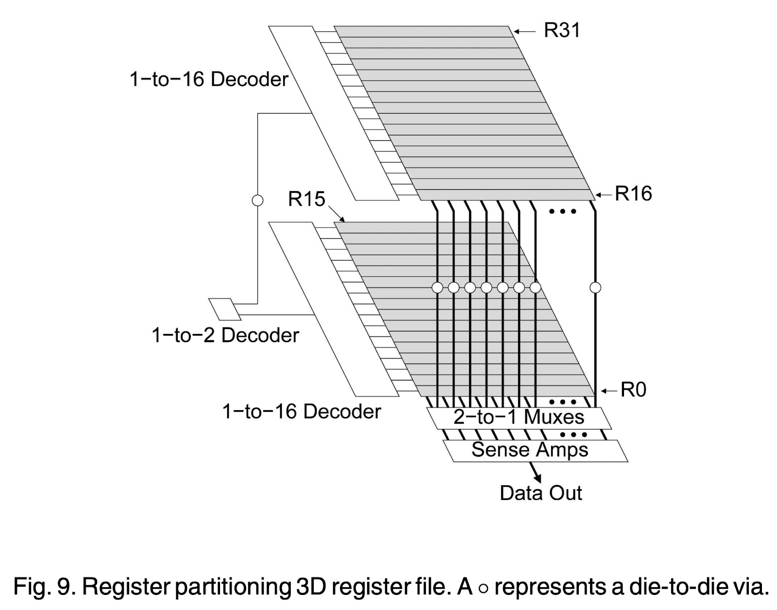
Fig. 68, Source: 3D-Integrated SRAM Components for High-Performance Microprocessors | IEEE Journals & Magazine
There are two main routes this could happen:
Route 1: Small TSVs (through-silicon vias)
Transistor layers manufactured separately on separate wafers, and bonded and connected together with TSVs
Route 2: Monolithic 3D
Transistors grown on top of each other layer by layer, on a single wafer
Fig. 69, Source: IFTLE 459: imec Develops Nano-TSV for Heterogeneous Integration - 3D InCites

Fig. 70, Source: Design Challenges and Solutions for Ultra-High-Density Monolithic 3D ICs
Fig. 69 shows Imec research on nano-TSV based integration, Route 1.
Fig. 70 by contrast, shows Route 2, monolithic 3D based fine-grained 3D integration.
Physical Design Optimizations
Currently physical design is done at the standard cell level for most chips. However, an alternative is “full custom” chip design- which uses custom circuits and layouts at the transistor level to improve PPA (power, performance and area).
Can this bring big wins? For optimized tiled designs like bitcoin mining or AI chips, likely the answer is no.
In addition, although transistor level physical design would give us better density, it’s not clear that they would be able to reduce power, which is our entire problem (although they might, by reducing wire length).
One interesting idea though is co-optimizing the process and circuit block. This has already been done with SRAM for a very long time, but as the number of unique circuit blocks that matter for PPA decreases this might be useful to do for logic circuit blocks. Eg MAC units in an AI chip.
Conclusion (Chip Level)
To conclude, at a chip level, there are significant gains possible, on the order of ~3X*, mostly driven by 3D chips and new higher density memories allowing for smaller wires in register files and scratchpads.
*For some workloads.
System Level
The Opportunity
The most interesting workloads of our time (AI) run on many, many chips all connected together. The chip today is only a small instrument in the orchestra that is a modern computer system.
Today’s logic chips are connected to large amounts of memory, to other chips, cables, switch chips and more.
This is especially true for AI clusters with thousands (and in the future, millions- see project Stargate!) of interconnected chips.
At this level there are many opportunities, and the system level may very well be the biggest driver of performance improvements.
Let’s take an example, Nvidia’s NVL72:

Fig. 71, Source: This is the NVIDIA DGX GB200 NVL72 - ServeTheHome
Nvidia’s NVL72 system is a system built to target higher power densities per rack. This allows “packaging”* together many GPUs much closer, allowing for the use of cheap and more energy efficient short-haul copper cables instead of optics.
Nvidia reports this saved 20kW for a 125 kW system. The cost savings were likely even higher- many systems of this type can be dominated by the cost of cables!
*”packaging” in this case refers not to chip-level packaging, but packaging in the supercomputer sense- how boards and cables are connected together in a datacenter.
Photonics
Photonics has the potential to connect together many chips and memories with very low energy and capital cost.
Since we’ve seen before that the energy and capital cost of the interconnect can often dominate system costs, photonics could also offer the opportunity to be revolutionary in this regard.

Fig. 72, Source: Ref, Main 12
Today of course, we are far from that potential, with optics being the more expensive option. As economies of scale and additional research is put into photonics, it will likely eventually replace copper for the vast majority of inter-chip interconnects in the long run though.
Photonics also offers the opportunity for unique systems designs, such as disaggregated systems, which can allow for mix and matched memory to compute ratios (Fig. 72).
Since memory costs are often the dominant capital cost factor in AI systems (e.g. HBM costs dominate a H100 or MI300’s manufacturing costs), this could also greatly reduce capital costs.
However, while this would be revolutionary for memory bound workloads, this doesn’t do much for compute-bound workloads.
Memory
Memory innovations can also have cluster-level impacts.
As an example, the Calculon paper shows that having a large memory can greatly increase the throughput for AI training under a fixed cost budget (Fig. 73).
Fig. 73, Source: Ref, Main 13
Although in Calculon’s case they use an existing memory technology and don’t need a new technology, it still demonstrates the potential of system-level impacts of new memory technologies.
Nvidia GPUs
As a sidenote, these calculations exclude profit margins, Nvidia’s GPUs are known for having 90%+ profit margins, which skews the economic calculations. Capex becomes far more important than power when this happens for instance.
Much of this article says:
Computing costs are dominated by energy costs, not chip capex
The fully burdened energy costs
So reducing the cost of computing means increasing energy efficiency
There isn’t really a good way to do that, so that’s the limiting factor
The high margins on nvidia GPUs make assertion #1 incorrect for today’s end users- so this article is kind of useless to current end users of AI compute unless nvidia’s margins go down!
Chiplets
I’ve left aside a section for chiplets only to point out that:
they at best match Moore’s Law, not exceed it
Chiplets are useful for three reasons:
Improving yields
Smaller chips yield better, and thus have lower cost.
Instead of 1 big chip, have 4 small chips that have better yield in aggregate.
Again, this is at best matching Moore’s Law, those 4 chips do no better than 1 big chip.
Fault-tolerant designs like Cerebras or yield-harvesting approaches like nVidia GPUs greatly mitigate the benefits of chiplets for this use case.
Customizability and reuse
Lower NRE
This isn’t relevant directly to the technical aspects of performance limits, although they may be very relevant from a practical perspective.
Components that don’t scale with process node
Analog circuits like SERDES often don’t scale, and an eg 16nm SERDES might be the same size as a 7nm SERDES, which makes it a waste to spend expensive 7nm die area on a circuit that hasn’t gotten smaller.
Again, this is at best matching, full swing Moore’s Law would scale the SERDES at the same rate as logic, which would make chiplets a moot point.
The big driver here might be SRAM, since SRAM did not scale from 5nm to 3nm and it’s not expected to scale well in the future. This might motivate chip companies to put SRAM (especially in last layer caches) into a separate SRAM chip on an older node like 5nm.
Intel has done in the past with eDRAM, and AMD is now doing it too.
But, they also come with challenges:
Overhead
We’ve already seen how wires between circuit blocks can be expensive, even on-chip. Now imagine having to use big, slow off-chip wires that are energy expensive to connect them together!
Yield issues in the packaging
This can be especially challenging if an expensive part like an HBM stack has to be thrown away because a SERDES chiplet failed to bond.
Redundancy can be used to mitigate this, but that calls into question the benefits of chiplets in the first place!
For example, Intel’s EMIB daisy chaining was rumored to have yield issues.
Unconventional Computing
Cryogenic Computing
Cryogenic computing could break many of the limits highlighted above.
First, sub-thermionic operation isn’t necessary since lower temperatures mean that the Boltzmann limit, as a function of kT, allows for lower subthreshold swings than 60mV/dec.
Second, many new technologies like superconducting wires, new device types (e.g. josephson junction devices), small capacitor DRAMs (leakage becomes ~0) can be used, all of which result in a huge boost.
New degrees of freedom also potentially open up the cost of the cryogenic cooling system starts to dominate the total cost of ownership, which could allow for higher wafer prices and the use of more exotic materials.
Unfortunately, the extremely high cost and low efficiency of cryogenic cooling likely means that it’s not viable for now, at prices >50X that of a single wafer’s cost (Ref. Cryogenic Computing, 1).
This however, may change, with advances in reducing the cost (and maybe even the efficiency) of cryocoolers.
Cryocoolers also tend to become cheaper the larger they are, so a single gigantic cryocooler to service an entire 20 MW datacenter could be a lot cheaper. These could even be mass produced, with thousands of datacenters each requiring one across the world.
In summary, cryogenic computing could be a wildcard technology that would be revolutionary, but in order for this to happen, costs need to dramatically drop for cryocoolers.
Analog Computing
Analog computing has been hyped as a future computing paradigm, especially for AI compute workloads. The intuition put forth is that “analog computation is noisy but very efficient, but neural networks are intrinsically noisy, so analog should work”.
Unfortunately, what is often neglected in these cases is the conversion from the digital to the analog domain, which takes an enormous amount of energy and is also slow!
(Ref. Analog, 1 and 4)

Fig. 74, Source: Ref. Analog, 1
Fig. 74 from a benchmarking paper shows that when you account for the conversion energy from analog to digital (ADCs/DACs), analog computing ends up being a lot less energy efficient than digital.
The other problem is that digital approaches are already trading accuracy for performance in a way, by quantization! Further going down this path may bring unknown model quality degradation. Not to mention the difficulty of debugging such a system- is the problem an issue in the code, the idea itself or too much analog noise?
Finally, one thing worth noting is that analog approaches are generally proposed only for the matrix multiply (or convolution) parts of the computation, which is assumed to be the entirety of the computation (it generally is 90%+ of the workload). The linearity of these operations also often makes it possible to use things like error correcting codes and other compensation methods to maintain accuracy (to some degree).
However, other parts of the computation can often become the next bottleneck, e.g. softmax and layernorm. These operations are often both done in high precision and are nonlinear, making it very hard for analog to work well.
Reversible Computing
Computing has a fundamental lower limit to how energy efficient it can be. Each bit has a physically fundamental cost of kT*ln(2), where k is the Boltzmann constant.
This is known as Landauer’s Limit.
Upon closer inspection however, this fundamental cost of computing is not in computing itself, but the dissipation of a bit of information to the external environment.
If we keep a constant number of bits in the computing system, and ensure that we can recover the previous states (reversibility), then we can actually compute with lower energy than Landauer’s Limit!
(The history of Landauer’s Principle is fascinating, and has a long and deep connection to physics, to Maxwell’s Demon, Szilard’s information engine and more! While it’s outside the scope of this article, I highly recommend you read about it)
Ref. Reversible Computing, 4
Reversible computing in practice essentially trades off speed for power by operating slower but at less energy.
Unfortunately, the area and other overheads of this make it so that the immediate tradeoff is spending many times more delay than you get back. Eg for adiabatic logic the energy cost is (R * C^2 * V^2)/time, which means a constant energy cost of 2 * RC before you start to trade off the time for reduced energy. Not to mention the area overhead of the trapezoidal waveform generators.
This likely means that at least for the foreseeable future, adiabatic/reversible computing is not economically viable. A comparison point would be low-voltage CMOS, which also is much slower, for lower energy.
In addition, fully reversible computing means changing code and algorithms. While this might be viable for certain workloads like AI or HPC, this is unreasonable for general purpose code. Arguably, if changing code is a requirement, much greater gains can be made simply by writing more efficient code!
There is maybe the possibility of exploiting faster transistors (e.g. high mobility FETs or Mott-FETs w/ 100fs switching times) to counteract the speed losses of reversible computing. This extra speed could otherwise not be used in irreversible computing due to the power limit.
Reversible computing may also be able to exploit steep slope switches like Mott FETs and impact ionization FETs that operate at high voltages (since EnergyOfSignal != EnergyDissipated in reversible computing).
Certain microarchitectures could also offer extremely deep pipelines and therefore very high clock speeds, which reversible computing may also be able to exploit. Eg Intel’s NetBurst targeted 10GHz, and test chips were built to reach that. These were abandoned in part due to power limits, which reversible computing could overcome.
Real test chips running at 5 GHz at 130nm were made, but used custom circuits like domino logic and annihilation gates (Ref. Reversible Computing, 2). But, there are tradeoffs, e.g. adding more pipeline registers increases the energy.
More speculatively, there might be longer term approaches that could be revolutionary, especially with the decline of general purpose computing. For example, self-assembly methods could greatly reduce the cost per transistor, and even if each transistor is of very poor quality (low energy efficiency), that may be okay for reversible computing. Another option could be self assembled NEMS and molecular computing devices.
Fluctuation Computing
A number of computing approaches rely upon harnessing the noise in a system as fluctuations to efficiently implement probabilistic computing.
Two startups, Normal Computing and Extropic (Ref. Fluctuation Computing, 4,5) are attempting to commercially develop this technology.
Broadly, the idea is to directly model a probability distribution with the stochastic component provided by the hardware instead of digitally computing and storing the distribution.
This idea was proposed by Richard Feynman long ago (Ref. Fluctuation Computing, 3).
These are broadly grouped into “fluctuation computing”, and different proposals use different approaches, e.g. thermal noise, flicker noise, quantum tunneling effects, etc (Ref. Fluctuation Computing, 1,2).
These approaches can be used to implement probabilistic graphical models directly in hardware and run inference on them “at the speed of thermodynamics”- by exploiting the random fluctuations.
Currently these approaches are only useful for these types of graphical models, and other random sampling problems. These are useful for things like error correcting codes, and thus have immediate utility in RF channel coding applications and NAND flash controllers, but so far this algorithm class hasn’t been broadly used.
Lyric Semiconductor (Ref. Fluctuation Computing, 6) also tried something similar, but appears to have pivoted to an analog computing approach, as far as I can tell from their patents.
Conclusion
The big bottleneck going forward is likely to be power, since transistor density can increase ~100X in 2D, and ~10X in 3D. However, energy efficiency is likely to saturate around 10-20X, with the Boltzmann Limit setting the limit. Currently no viable candidate exists to be lower energy at a reasonable speed, which is a key area where we could use a breakthrough!
Memory-bound workloads are likely to see a big improvement, with orders of magnitude possible, but compute-bound workloads are running into a wall much faster.
End to End Pathfinding?
One interesting takeaway from this exercise has been that many of the figures of merit that each engineer gets at their layer of the stack is not necessarily what is actually the correct target.
For example, transistor device physicists are told to increase the speed of transistors, but more speed doesn’t necessarily help you if your cost of compute is bound by power consumption!
To make things more interesting, there are interactions between different layers of the stack.
For example, although increasing the transistor speed won’t help your cost of compute (on a per-chip basis) since energy dominates the cost of compute, increased transistor speed may increase the per-chip speed, reducing the number of chips and therefore cables.
Thus, even though per-chip compute cost is not reduced, system-level compute cost is reduced.
Deepflow is an example of a smaller scope attempt of doing this, see below:

Foundry pathfinding may need to shift to a similar end to end approach, to maximize the performance gains from an increasingly harder device physics problem.
References
Main
A Kinder and Gentler Tour to Computer Architecture Research - ppt download
[1207.6819] Device Considerations for Nanophotonic CMOS Global Interconnects
https://ieeexplore.ieee.org/stamp/stamp.jsp?arnumber=8472140
Calculon: a methodology and tool for high-level co-design of systems and large language models
CMOS Scaling
Is there a Fundamental Limit to Miniaturizing CMOS Transistors?
Saving Moore’s Law Down To 1 nm Channels With Anisotropic Effective Mass | Scientific Reports
VTFET: IBM's revolutionary new chip architecture | IBM Research Blog
Advanced MOSFET Structures and Processes for Sub-7 nm CMOS Technologies
Vertical GAAFETs for the Ultimate CMOS Scaling | IEEE Journals & Magazine
IEDM 2017 + ISSCC 2018: Intel’s 10nm, switching to cobalt interconnects – Page 6 – WikiChip Fuse
Design of ion-implanted MOSFET's with very small physical dimensions
VTFET: IBM’s revolutionary new chip architecture | IBM Research Blog
https://nanohub.org/resources/35870/download/Fundamentals_of_Nanotransistors.pdf
IEDM 2022: Did We Just Witness The Death Of SRAM? – WikiChip Fuse
SRAM Assist Techniques for Operation in a Wide Voltage Range in 28-nm CMOS
imec magazine September 2017 - The vertical nanowire FET: enabler of highly dense SRAMs
Cryogenic-DRAM based memory system for scalable quantum computers: a feasibility study
Tiered-Latency DRAM: A Low Latency and Low Cost DRAM Architecture
Highly scaled SOT-MRAM: low switching energy, high endurance | imec
X
Direct S-D Tunneling
Vertical FETs
Manufacturing
Economics
Economics of 3D
Enhanced CMOS
Negative Capacitance
Is negative capacitance FET a steep-slope logic switch? | Nature Communications
[1903.03884] A Critical Review of Recent Progress on Negative Capacitance Field-Effect Transistors
X
TFETs
Energy Filtering
2D TMDs
Process integration and future outlook of 2D transistors | Nature Communications
Two dimensional semiconducting materials for ultimately scaled transistors
Two dimensional semiconducting materials for ultimately scaled transistors - ScienceDirect
Transistors based on two-dimensional materials for future integrated circuits
Process integration and future outlook of 2D transistors | Nature Communications
X
III-Vs
Quantum capacitance in scaled down III–V FETs | IEEE Conference Publication
https://ieeexplore.ieee.org/abstract/document/7855831/authors#authors
Carbon Nanotubes
Z
Tunneling FETs
Beyond CMOS
[1302.0244] Overview of Beyond-CMOS Devices and A Uniform Methodology for Their Benchmarking
Materials and Devices beyond CMOS Transistor for Energy Efficient Computing
Benchmarking of Beyond-CMOS Exploratory Devices for Logic Integrated Circuits
X
Spintronics
NEMS
Cryogenic Computing
Reversible Computing
5-GHz 32-bit integer execution core in 130-nm dual-V/sub T/ CMOS
The Reversible Computing Scaling Path: Challenges and Opportunities
https://www.sandia.gov/app/uploads/sites/210/2023/10/Comet23-slides-topost.pdf
X
Analog
Analog/Mixed-Signal Hardware Error Modeling for Deep Learning Inference
https://ieeexplore.ieee.org/stamp/stamp.jsp?arnumber=9598887
https://cds.cern.ch/record/2199013/files/arXiv:1607.01704.pdf
[2308.01719] The Data Conversion Bottleneck in Analog Computing Accelerators
Fluctuation Computing
Chip-Level
AI Chips
X
Tapa you're insane, excited to read through this :D